- 您现在的位置:买卖IC网 > Sheet目录3874 > PIC16LF724-E/PT (Microchip Technology)IC PIC MCU FLASH 7KB 44-TQFP
2009 Microchip Technology Inc.
DS41341E-page 105
PIC16F72X/PIC16LF72X
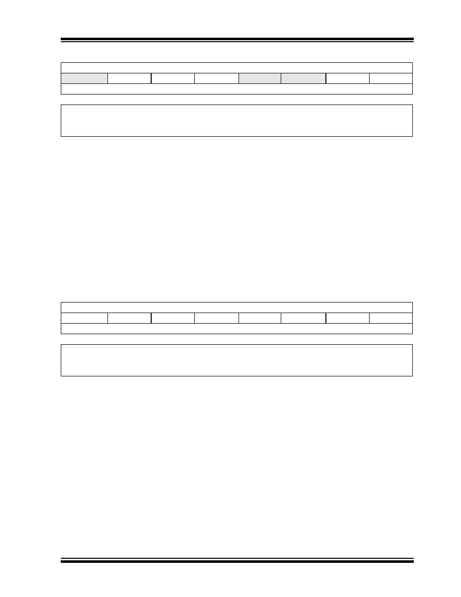
REGISTER 9-2:
ADCON1: A/D CONTROL REGISTER 1
REGISTER 9-3:
ADRES: ADC RESULT REGISTER
U-0
R/W-0
U-0
R/W-0
—
ADCS2
ADCS1
ADCS0
—
ADREF1
ADREF0
bit 7
bit 0
Legend:
R = Readable bit
W = Writable bit
U = Unimplemented bit, read as ‘0’
-n = Value at POR
‘1’ = Bit is set
‘0’ = Bit is cleared
x = Bit is unknown
bit 7
Unimplemented: Read as ‘0’
bit 6-4
ADCS<2:0>: A/D Conversion Clock Select bits
000
=FOSC/2
001
=FOSC/8
010
=FOSC/32
011
=FRC (clock supplied from a dedicated RC oscillator)
100
=FOSC/4
101
=FOSC/16
110
=FOSC/64
111
=FRC (clock supplied from a dedicated RC oscillator)
bit 3-2
Unimplemented: Read as ‘0’
bit 1-0
ADREF<1:0>: Voltage Reference Configuration bits
0x
=VREF is connected to VDD
10
=VREF is connected to external VREF (RA3/AN3)
11
=VREF is connected to internal Fixed Voltage Reference
R/W-x
ADRES7
ADRES6
ADRES5
ADRES4
ADRES3
ADRES2
ADRES1
ADRES0
bit 7
bit 0
Legend:
R = Readable bit
W = Writable bit
U = Unimplemented bit, read as ‘0’
-n = Value at POR
‘1’ = Bit is set
‘0’ = Bit is cleared
x = Bit is unknown
bit 7-0
ADRES<7:0>: ADC Result Register bits
8-bit conversion result.
发布紧急采购,3分钟左右您将得到回复。
相关PDF资料
PIC18LF44J10T-I/ML
IC PIC MCU FLASH 8KX16 44QFN
PIC16LF727-I/PT
IC PIC MCU FLASH 8K 1.8V 44-TQFP
PIC24F08KA102-I/SO
IC PIC MCU FLASH 8K 28-SOIC
PIC18LF44J10T-I/PT
IC PIC MCU FLASH 8KX16 44TQFP
PIC24F16KL401-I/SO
IC MCU 16BIT 16KB FLASH 20-SOIC
PIC18LF25J10T-I/SS
IC PIC MCU FLASH 16KX16 28-SSOP
PIC16LF1527-I/PT
MCU PIC 28KB FLASH 64TQFP
PIC18F25K20-I/SP
IC PIC MCU FLASH 16KX16 28-DIP
相关代理商/技术参数
PIC16LF724-I/ML
功能描述:8位微控制器 -MCU 7KB Flash Prog 16MHz Int Osc 1.8V-5.5V
RoHS:否 制造商:Silicon Labs 核心:8051 处理器系列:C8051F39x 数据总线宽度:8 bit 最大时钟频率:50 MHz 程序存储器大小:16 KB 数据 RAM 大小:1 KB 片上 ADC:Yes 工作电源电压:1.8 V to 3.6 V 工作温度范围:- 40 C to + 105 C 封装 / 箱体:QFN-20 安装风格:SMD/SMT
PIC16LF724-I/MV
功能描述:8位微控制器 -MCU 7KB Flash RAM 192b nanoWatt RoHS:否 制造商:Silicon Labs 核心:8051 处理器系列:C8051F39x 数据总线宽度:8 bit 最大时钟频率:50 MHz 程序存储器大小:16 KB 数据 RAM 大小:1 KB 片上 ADC:Yes 工作电源电压:1.8 V to 3.6 V 工作温度范围:- 40 C to + 105 C 封装 / 箱体:QFN-20 安装风格:SMD/SMT
PIC16LF724-I/P
功能描述:8位微控制器 -MCU 7KB 1.8-3.6V 16MHz 8b ADC CCP Lo Pwr
RoHS:否 制造商:Silicon Labs 核心:8051 处理器系列:C8051F39x 数据总线宽度:8 bit 最大时钟频率:50 MHz 程序存储器大小:16 KB 数据 RAM 大小:1 KB 片上 ADC:Yes 工作电源电压:1.8 V to 3.6 V 工作温度范围:- 40 C to + 105 C 封装 / 箱体:QFN-20 安装风格:SMD/SMT
PIC16LF724-I/PT
功能描述:8位微控制器 -MCU 7KB 1.8-3.6V 16MHz 8b ADC CCP Lo Pwr
RoHS:否 制造商:Silicon Labs 核心:8051 处理器系列:C8051F39x 数据总线宽度:8 bit 最大时钟频率:50 MHz 程序存储器大小:16 KB 数据 RAM 大小:1 KB 片上 ADC:Yes 工作电源电压:1.8 V to 3.6 V 工作温度范围:- 40 C to + 105 C 封装 / 箱体:QFN-20 安装风格:SMD/SMT
PIC16LF724T-I/ML
功能描述:8位微控制器 -MCU 7KB Flash Prog 16MHz Int Osc 1.8V-5.5V
RoHS:否 制造商:Silicon Labs 核心:8051 处理器系列:C8051F39x 数据总线宽度:8 bit 最大时钟频率:50 MHz 程序存储器大小:16 KB 数据 RAM 大小:1 KB 片上 ADC:Yes 工作电源电压:1.8 V to 3.6 V 工作温度范围:- 40 C to + 105 C 封装 / 箱体:QFN-20 安装风格:SMD/SMT
PIC16LF724T-I/MV
功能描述:8位微控制器 -MCU 7KB Flash RAM 192b nanoWatt RoHS:否 制造商:Silicon Labs 核心:8051 处理器系列:C8051F39x 数据总线宽度:8 bit 最大时钟频率:50 MHz 程序存储器大小:16 KB 数据 RAM 大小:1 KB 片上 ADC:Yes 工作电源电压:1.8 V to 3.6 V 工作温度范围:- 40 C to + 105 C 封装 / 箱体:QFN-20 安装风格:SMD/SMT
PIC16LF724T-I/PT
功能描述:8位微控制器 -MCU 7KB Flash Prog 16MHz Int Osc 1.8V-5.5V
RoHS:否 制造商:Silicon Labs 核心:8051 处理器系列:C8051F39x 数据总线宽度:8 bit 最大时钟频率:50 MHz 程序存储器大小:16 KB 数据 RAM 大小:1 KB 片上 ADC:Yes 工作电源电压:1.8 V to 3.6 V 工作温度范围:- 40 C to + 105 C 封装 / 箱体:QFN-20 安装风格:SMD/SMT
PIC16LF726-E/ML
功能描述:8位微控制器 -MCU 14KBFlash Prog 16MHz Int Osc 1.8V-5.5V
RoHS:否 制造商:Silicon Labs 核心:8051 处理器系列:C8051F39x 数据总线宽度:8 bit 最大时钟频率:50 MHz 程序存储器大小:16 KB 数据 RAM 大小:1 KB 片上 ADC:Yes 工作电源电压:1.8 V to 3.6 V 工作温度范围:- 40 C to + 105 C 封装 / 箱体:QFN-20 安装风格:SMD/SMT